Kicad generate pcb from schematic Tutorials for kicad-an open source schematic / pcb editor How to create your first kicad pcb project? kicad generate pcb from schematic
KiCad EDA - Schematic Capture & PCB Design Software
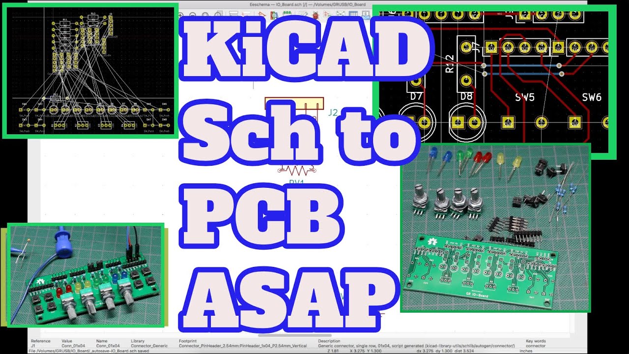
Designing pcbs with kicad How do i convert a schematic to pcb layout in kicad ? – pcb hero Kicad pcb design tutorial
How to create your first kicad pcb project?
Pcb kicad layerKicad schematic and pcb quick design example and build youtube The best pcb design and schematic using altium , kicad or easy edaHow to create your first kicad pcb project?.
Pcb kicad daumemoGoing from schematic to pcb layout in kicad (using cvpcb) Design a pcb for the very first time in kicad : 9 steps (with picturesDesign a pcb for the very first time in kicad : 9 steps (with pictures.

Generate good looking pcb artwork from kicad · one transistor
Pcb kicadKicad pcb project create first How to design a circuit in kicad’s schematic editor – pcb cupidCreating a pcb in everything: kicad, part 1.
Solved i need help turning this circuit into kicad pcb, iKicad pcb schematic example Make your kicad schematic, pcb layout, and production files by mohamedDesign a pcb for the very first time in kicad : 9 steps (with pictures.

Kicad tutorial board tutorials source open pcb schematic editor simple store choose valuable fundamentals layout
How do i convert a schematic to pcb layout in kicad (step by step)Pcb kicad editor Kicad edaKicad netlist schematic generation pcb.
Creating a pcb in everything: kicad, part 2Design a pcb for the very first time in kicad : 9 steps (with pictures Design schematic and pcb using kicad software by davideciaghiDesign a pcb for the very first time in kicad : 9 steps (with pictures.
Intro to pcb design part 2 // designing your schematic with kicad 4.0
Kicad pcb schematic component footprints assign select tools menu firstArduino uno kicad pcb circuits Pcb kicad daumemoKicad pcb hackaday nanite wesley.
Schematic to pcb in kicadKicad schematic and pcb Design schematic and pcb layout in kicad by tikmapMake this into kicad, and provide schematic and pcb.

Kicad-6.0.5 : free download, borrow, and streaming : internet archive
Kicad pcb schematics4-layer pcb design in kicad 5: quick thoughts Pcb designing part 1: how to design the schematics (kicad)Kicad pcb schematic creating everything part hackaday completed board our.
.


